- 您现在的位置:买卖IC网 > Sheet目录2040 > PI74FCT16245CTVEX (Pericom)IC TXRX 16BIT BIDIR 48SSOP
PI74FCT16245T
PI74FCT162245T
Fast CMOS 16-Bit Bidirectional Tranceivers
2
PS2032K
11/06/08
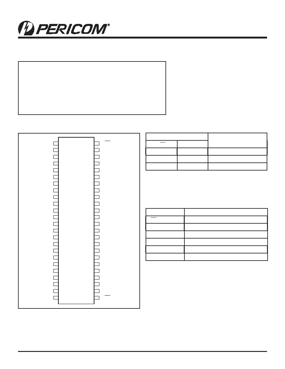
Pin Description
Pin Name
Description
XOE
3-State Enable Inputs (Active LOW)
XDIR
Direction Control Input
XAX
Side A Inputs or 3-State Outputs
XBX
Side B Inputs or 3-State Outputs
GND
Ground
VCC
Power
Truth Table
Inputs(1)
Outputs(1)
XOE
XDIR
L
Bus B Data to Bus A
L
H
Bus A Data to Bus B
H
X
High Z State
Note:
1.
H = High Voltage Level, X = Don’t Care,
L = Low Voltage Level, Z = High Impedance
Pin Conguration
1DIR
1B0
1B1
GND
1B2
1B3
VCC
1B4
1B5
GND
1B6
1B7
2B0
2B1
GND
2B2
2B3
VCC
2B4
2B5
GND
2B6
2B7
2DIR
1OE
1A0
1A1
GND
1A2
1A3
VCC
1A4
1A5
GND
1A6
1A7
2A0
2A1
GND
2A2
2A3
VCC
2A4
2A5
GND
2A6
2A7
2OE
1
2
3
4
5
6
7
8
9
10
11
12
13
14
15
16
17
18
19
20
21
22
23
24
48
47
46
45
44
43
42
41
40
39
38
37
36
35
34
33
32
31
30
29
28
27
26
25
Storage Temperature ............................................................ –65°C to +150°C
Ambient Temperature with Power Applied ........................... –40°C to +85°C
Supply Voltage to Ground Potential (Inputs & VCC Only).....–0.5V to +7.0V
Supply Voltage to Ground Potential (Outputs & D/O Only) ..–0.5V to +7.0V
DC Input Voltage ....................................................................–0.5V to +7.0V
DC Output Current............................................................................... 120mA
Power Dissipation ................................................................................... 1.0W
Note:
Stresses greater than those listed under MAXIMUM
RATINGS may cause permanent damage to the
device. This is a stress rating only and functional
operation of the device at these or any other con-
ditions above those indicated in the operational
sections of this specification is not implied.
Exposure to absolute maximum rating conditions for
extended periods may affect reliability.
Maximum Ratings
(Above which the useful life may be impaired. For user guidelines, not tested.)
08-0291
发布紧急采购,3分钟左右您将得到回复。
相关PDF资料
PI74FCT16245CTVE
IC TRANSCVR DUAL N-INV 48SSOP
PI74FCT244TSEX
IC BUFF/DVR OCTAL N-INV 20SOIC
PI74FCT245DTQE
IC TRANSCEIVER 8BIT N-INV 20QSOP
PI74FCT273TSE
IC OCTAL D F-F W/RESET 20-SOIC
PI74FCT3244S
IC BUFF DVR 8BIT N-INV 20SOIC
PI74FCT373TQE
IC OCTAL TRANSPARENT LTCH 20QSOP
PI74FCT374ATQE
IC OCT D REG 3-STATE 20 QSOP
PI74LCX16245AE
IC 16BIT BIDIR TXRX 3.3V 48TSSOP
相关代理商/技术参数
PI74FCT16245DTA
制造商:未知厂家 制造商全称:未知厂家 功能描述:Dual 8-bit Bus Transceiver
PI74FCT16245DTK
制造商:未知厂家 制造商全称:未知厂家 功能描述:Dual 8-bit Bus Transceiver
PI74FCT16245DTSP
制造商:未知厂家 制造商全称:未知厂家 功能描述:Dual 8-bit Bus Transceiver
PI74FCT16245DTV
制造商:未知厂家 制造商全称:未知厂家 功能描述:Dual 8-bit Bus Transceiver
PI74FCT16245ETA
制造商:未知厂家 制造商全称:未知厂家 功能描述:Dual 8-bit Bus Transceiver
PI74FCT16245ETK
制造商:未知厂家 制造商全称:未知厂家 功能描述:Dual 8-bit Bus Transceiver
PI74FCT16245ETV
制造商:未知厂家 制造商全称:未知厂家 功能描述:Dual 8-bit Bus Transceiver
PI74FCT16245T
制造商:PERICOM 制造商全称:Pericom Semiconductor Corporation 功能描述:Fast CMOS 16-Bit Bidirectional Transceivers